
Benchmark Technology Options for Your Designs
Be ahead of the curve – optimize your designs for future technologies
CMOS scaling beyond N7 has several contenders with potential to become the platform for the future technology nodes. On the one hand, there is the evolution of the FinFET technology towards gate-all-around devices, such as the stacked-nanowire-FET (NWFET) and the stacked-nanosheet-FET (NSFET), which aim to improve electrostatic control of the channel over the current bulk FinFET technology. Both technologies have already been demonstrated in hardware and both allow to retain the circuit design principles developed for the latest FinFET generation, making their adoption viable for the N5 node and beyond. On the other hand, there are more radical options such as the complementary FET (CFET) technology, a 3D integration technique which stacks NMOS and PMOS transistors on top of each other and moves the power supply rails to the FEOL. With a hardware realization yet to be demonstrated, the introduction of the CFET would allow the design of three and four-track cells thereby drastically reducing the cell size.
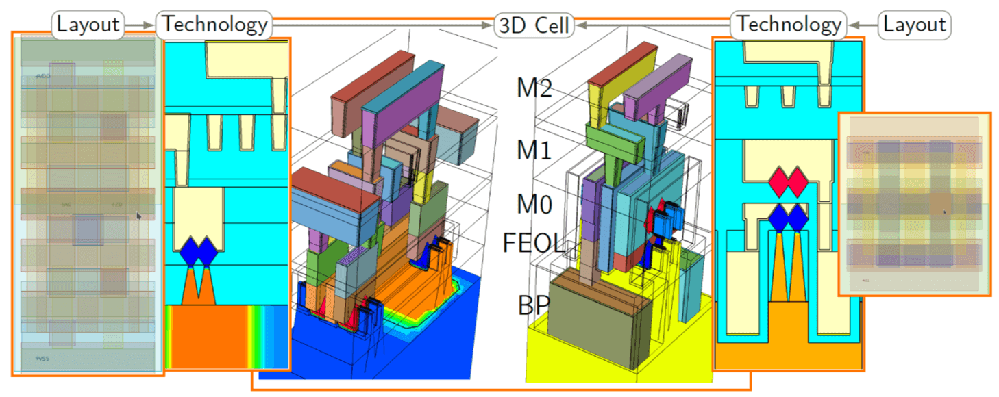
Deciding on a technology has big implications from device and cell to circuit and system level. With GTS Cell Designer you can benchmark technology options (FinFET, NWFET, NSFET, CFET, VFET, etc.) and get the best design for each.
Power Performance Area (PPA) of ring oscillators
One of the staple logic cells for assessment of a technology’s capabilities is the ring oscillator. For a given layout and technology a detailed 3D TCAD model can be built that captures the key figures of merit. By applying the GTS DTCO flow, one can perform steady-state, transient, thermal, and AC analyses to determine device characteristics, power/performance figures, self-heating properties, and parasitic resistances and capacitances, respectively. Quickly obtaining accurate power-performance-area data enables sensible path-finding for your designs. The consistent TCAD-based approach shown here integrates all necessary information regarding your front-end-of-line device performance, your middle-of-line parasitics and the interaction of all components in the logic cell. The flow can be easily extended to incorporate time-zero variability and ageing to complete the picture, thus putting your design and technology choices on a sound basis.

SRAM – driving your technology
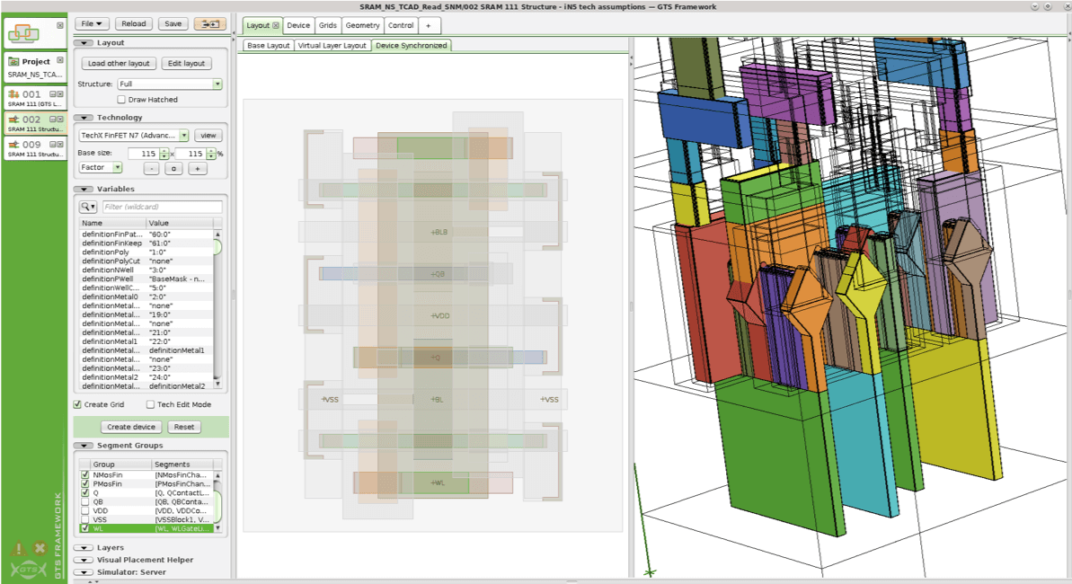
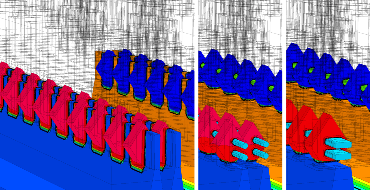
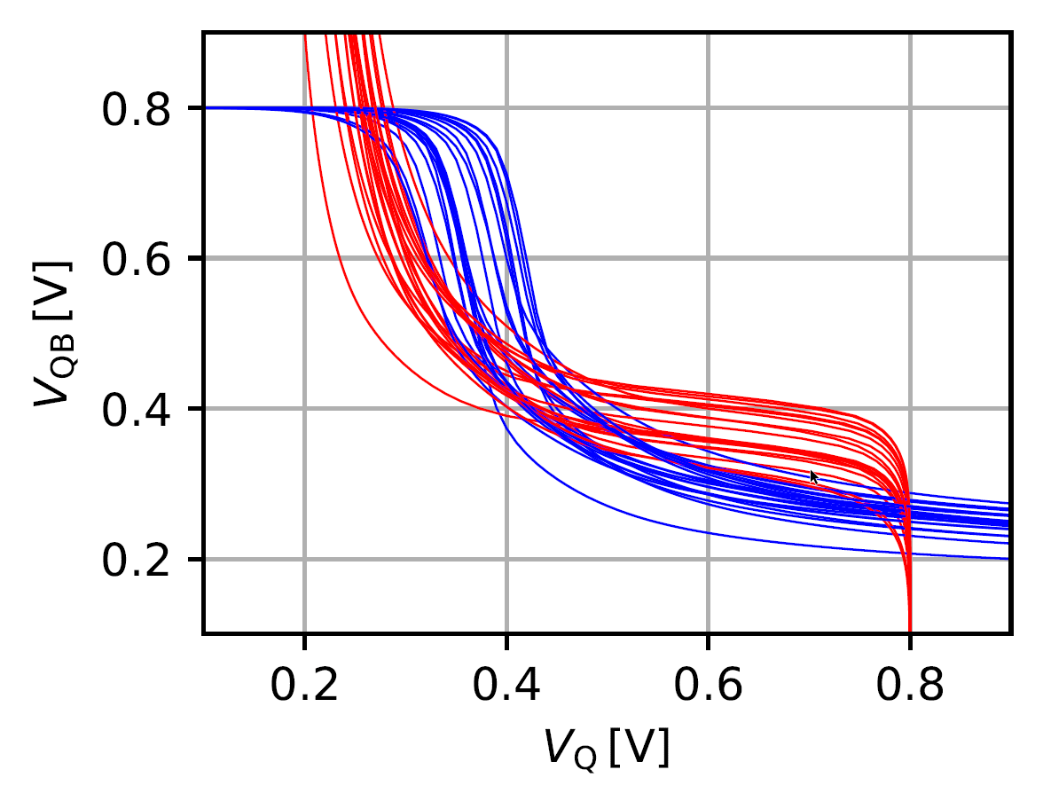
No other device shows the maturity of a technology better than the high-density SRAM. As such it poses critical challenges to all parties involved, with stringent requirements on proces and design. DTCO can help to smoothen the task and deliver crucial insights into the device and circuit performance. These can guide fundamental technology choices such as using FinFET, Nanosheet, or Nanowire devices for your platform. A holistic view of the SRAM cell using TCAD-based DTCO considers all relevant device and parasitics information to provide confidence in key figures of merit including Static Noise Margin (SNM), Write Trip Point (WTP), read/write current as well as bitline/wordline resistances and capacitances.
GTS Cell Designer allows to study the impact of variability including MGG, RDD, and LER on key SRAM metrics. Using our reliability-aware DTCO flow, ageing and variability can be systematically captured and addressed timely through mitigation approaches at the cell level.

GTS Cell Designer – implements a revolutionary sleek work flow for optimizing circuit designs for various technologies specifically, either without going into process details (LSG), or with the process included (ProEmu).
GTS ProEmu – a universal, module-based process emulator. Use flexible process modules to easily explore new designs. Study variability and optimize for device PPA as well as production yield. Understand how each process step affects subsequent steps as well as device performance. Tune your technology, leap ahead.