22. June 2021
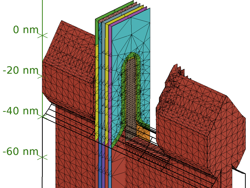
We are proud to announce the publication of our most recent paper in IEEE Transactions on Electron Devices (TED). The paper shows how we have taken TCAD device simulation to a new level with GTS Nano Device Simulator (NDS).
Initially released in 2015, NDS has evolved to become the standard tool for modeling carrier transport in nano-scale MOSFETs in both industry and academia. For the first time since its initial release, we publicly disclose details about NDS’ features and methods.
Nanoscale MOSFETs, Planar / Nonplanar – Path-Finding & DTCO
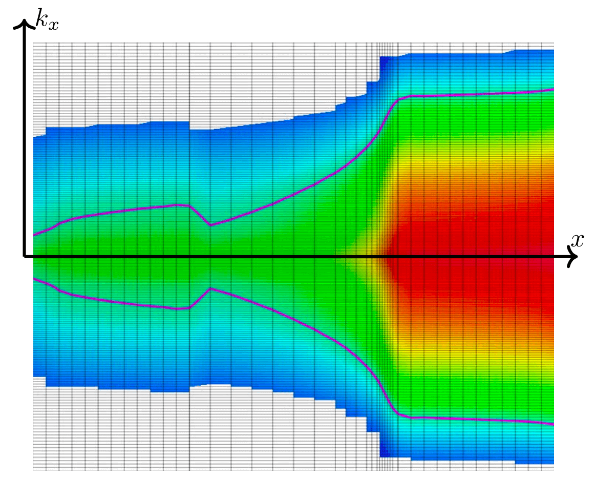
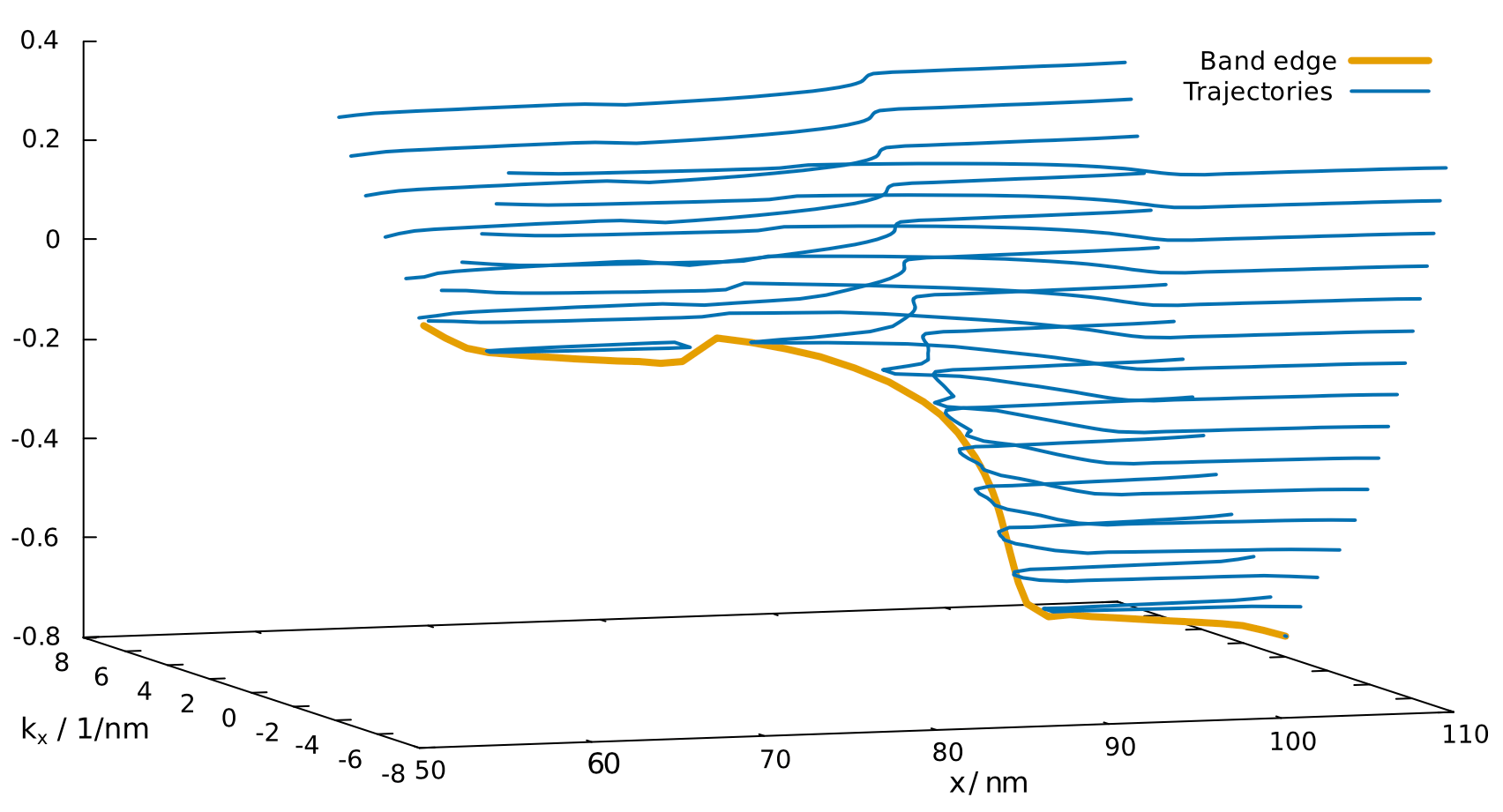
The paper presents a major update on the methodology behind GTS Nano Device Simulator (NDS), which is based on the subband Boltzmann transport equation (SBTE), and illustrates applications in simulation of nanoscale MOSFETs. It shows a wide range of applications SBTE is suited for, including state-of-the-art nonplanar and well-established planar technologies. See how SBTE can be employed both as a path-finding tool as well as a fundamental component in a DTCO-flow.
Precisely Predicting Device Performance by Physical Modeling
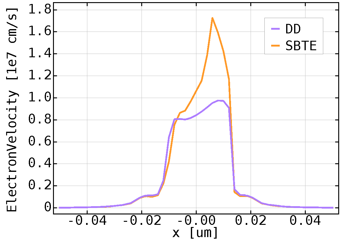
As an SBTE solver, NDS accurately models the effects of quantum confinement, crystal orientation, high values of mechanical stress, carrier scattering, and short-channel effects, such as velocity-overshoot, on device performance. It does that based on physics rather then fitted empirical models. Furthermore, NDS provides a platform for TCAD model building and a reference for the calibration of empirical and compact models.
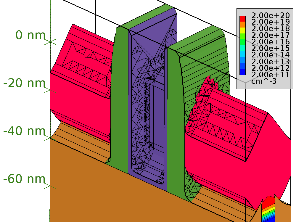
NDS has proven useful across multiple technologies including FinFET, stacked horizontal nanosheets and nanowires, vertical nanosheets and nanowires, as well as planar technologies, such as FDSOI and Bulk MOSFETs. In this paper, we provide an overview of the model details used in NDS and its extended use cases that go beyond the scope of previous publications.
Open Access Paper
We have chosen to make the paper available through Open Access because we feel it’s important to support the free exchange of ideas. The paper is available through IEEE Xplore (DOI:10.1109/TED.2021.3079884) – or you can download the paper at MyGTS.
If you want to know more about the applications of Nano Device Simulator go to pathfinding or DTCO, look at our product page and explore our application examples. Feel free to contact us directly for specific enquiries.

