3D Gate All-Around Vertical NAND Flash Memory

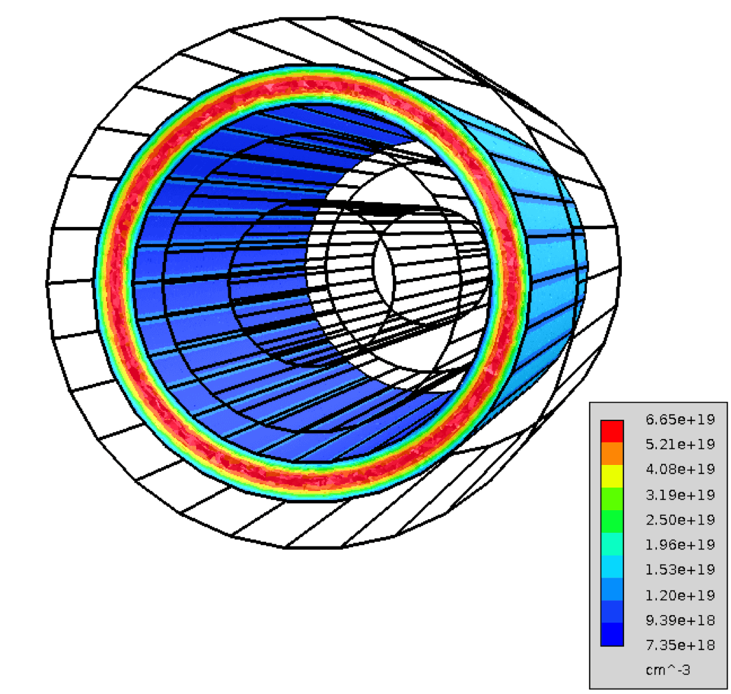
Trapping-based non-volatile memories (NVM) have developed into a central building block of modern data storage technology in recent years. The most dominant implementation of this technology today is cylindrical 3D gate all-around vertical NAND (VNAND) structures. Modeling these devices poses a challenge due to the imperfect re-crystallization of the silicon layer during production. This imperfect re-crystallization leads to the formation of multiple grains in the conducting layer which strongly impact the transconductive behavior.
Automated Workflows for Comprehensive R&D
GTS Framework is used at the forefront of V-NAND technology development. The software package offers automated workflows for the generation of realistic grain structures and a sophisticated combination of physical models that has been refined and verified by detailed comparison to experimental data. GTS also offers ready-to-run configurable examples for the simulation of common experimental setups, e.g. transconductance behavior, retention, write/erase, and ISPP, of full 3D multi-gate V-NAND structures.
Trans-Conductance
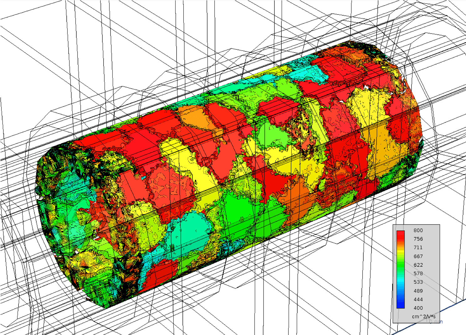
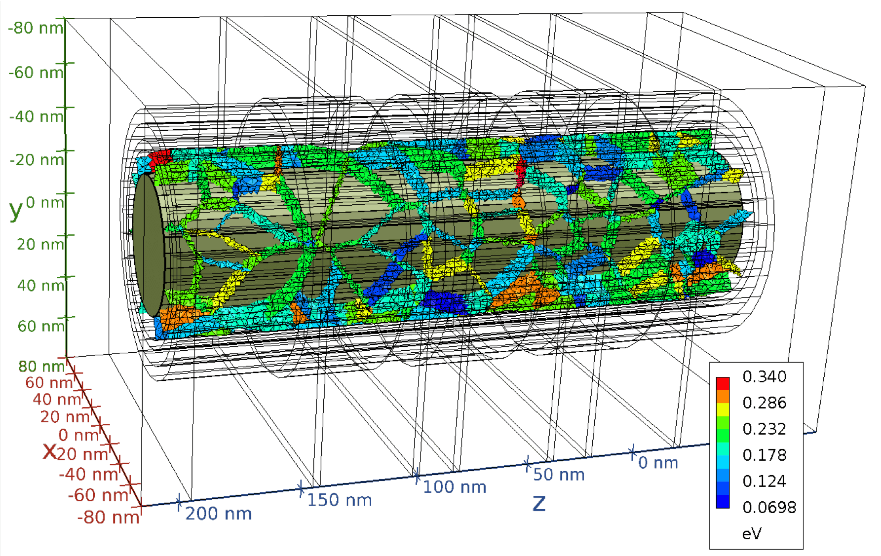
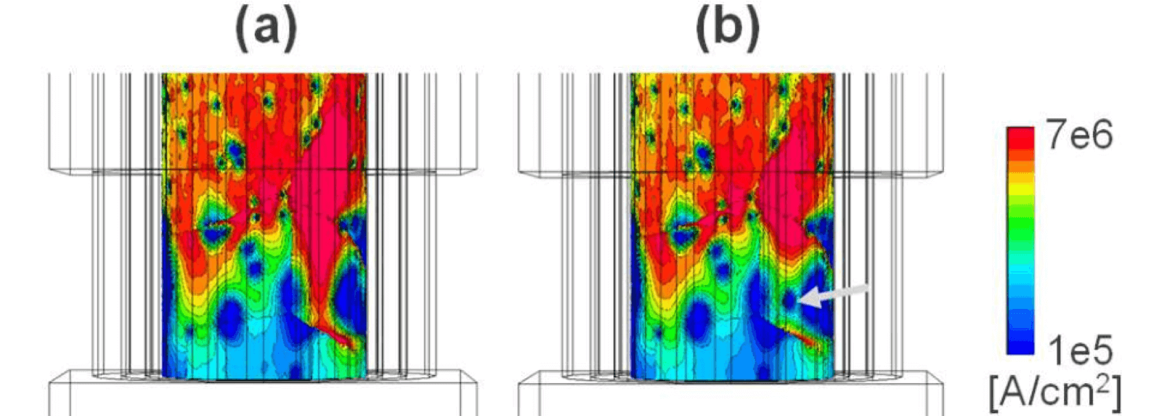
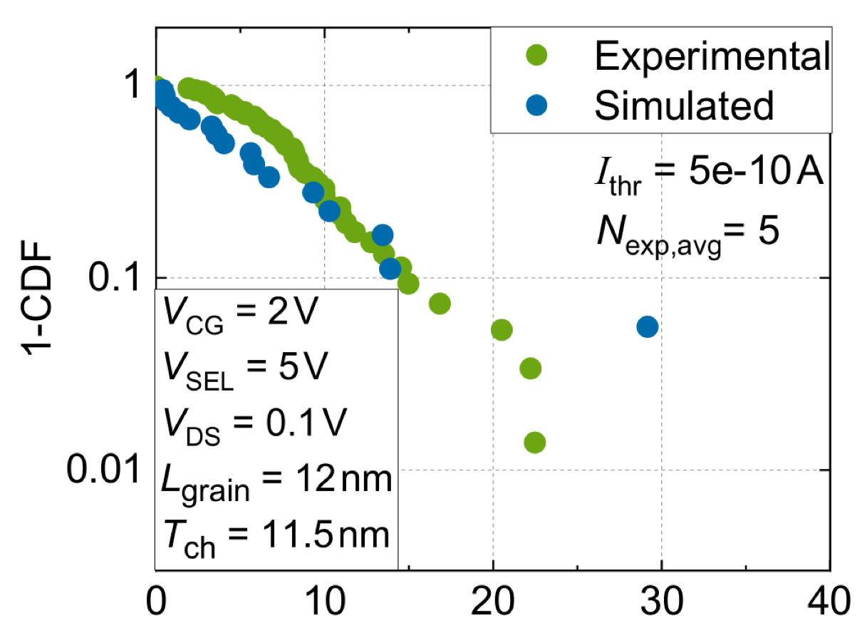
The transconductance of V-NAND devices shows complex device-to-device variability. This variability originates from the formation of silicon grains with varying crystal orientation in the conducting channel layer of the macaroni structure as well as from discrete traps.
Sophisticated modeling is used to explain the state-of-the-art experimental observations on V-NAND structures. The dependence of the carrier mobility on the grain orientation, mechanical stress, and gate bias, as well as increased scattering at the grain boundaries are considered to accurately model the on-current variability. Barrier hopping at the grain boundary is used to explain the temperature dependence of the on-state current when grains are present. Discrete traps at the grain boundaries are included to model the sub-threshold swing degradation.
Time-zero-variability as well as time dependent variability are captured in the physical models of GTS Minimos-NT and can be conveniently used in large scale statistical studies using the infrastructure provided by GTS Framework.
Random Telegraph Noise
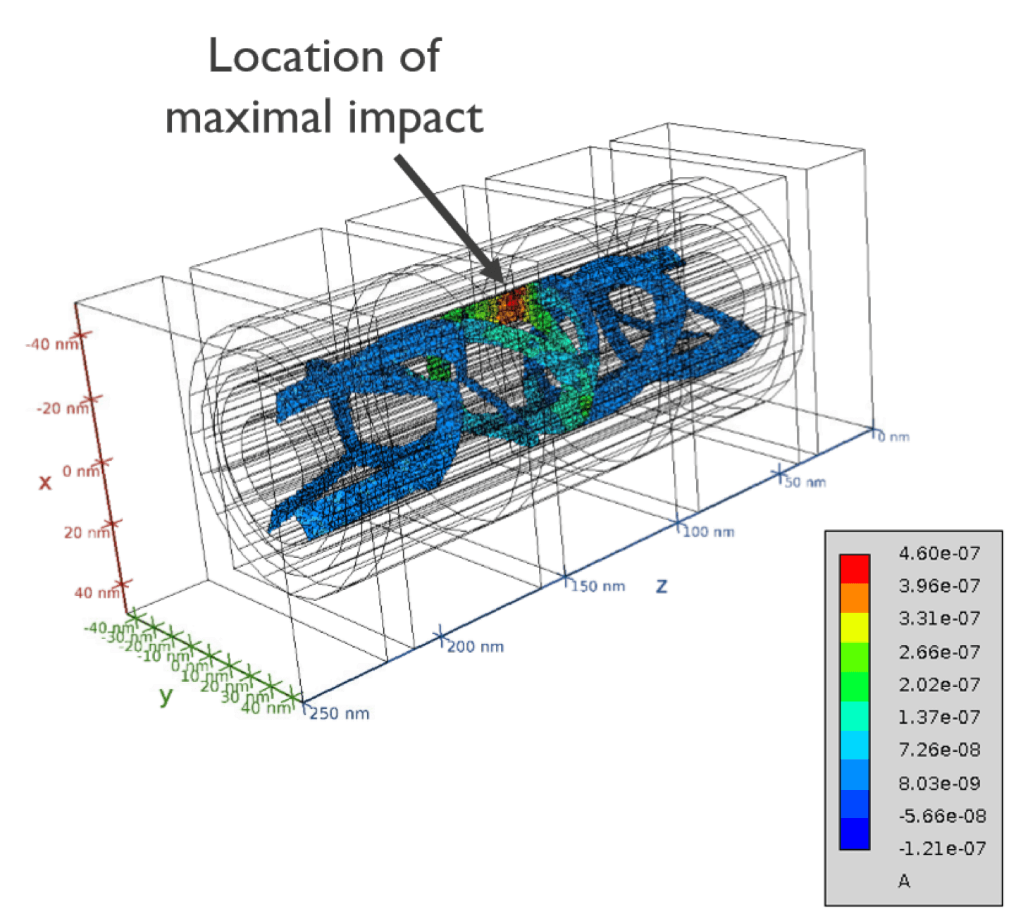
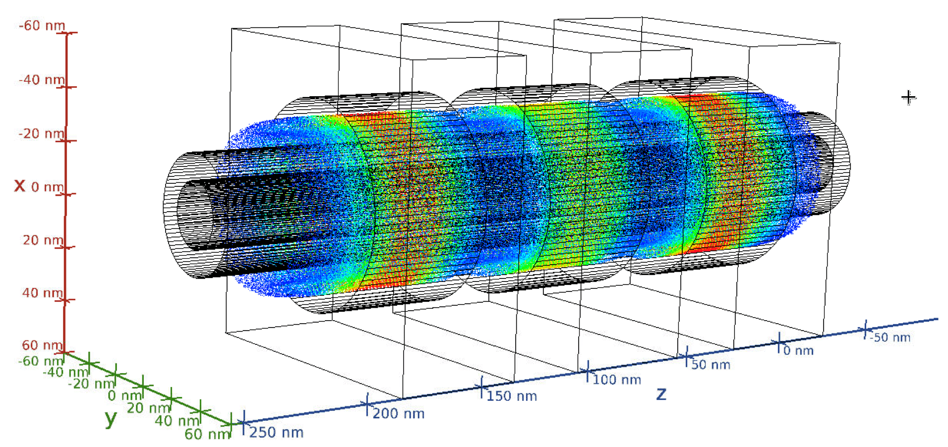
In addition to impacting the transconductance behavior, the charging and discharging of point defects in the poly-grain channel gives rise to random telegraph signals that impact the readout reliability of the devices. The GTS 3D TCAD simulator can efficiently determine the regions of increased vulnerability to traps in a device using a linear response method. It has been successfully used to model and explain large single-trap charge-induced VT-shifts obtained by measurements of GAA-VNAND devices.
Memory Operation
GTS Software is actively used for the simulation of the charging dynamics of flash memory technologies, both state-of-the-art and path-finding. GTS Minimos-NT offers physical models for various charge storage layers, including simple metal floating gates, NOR Flash polysilicon layers, and SONOS trapping layers.
Quantum mechanical tunneling through insulators can be calculated on realistic complex 3D geometries using the flexible and robust tunnel path placement algorithms.
GTS Minimos-NT features a state-of-the art dedicated model set for SONOS charge trapping layer dynamics consisting of
- a description of the free carrier motion in the trapping layer as a field-dependent hopping transport
- a non-uniform distribution of electrically active traps inside the trapping layer
- a dedicated trap to band tunneling emission model
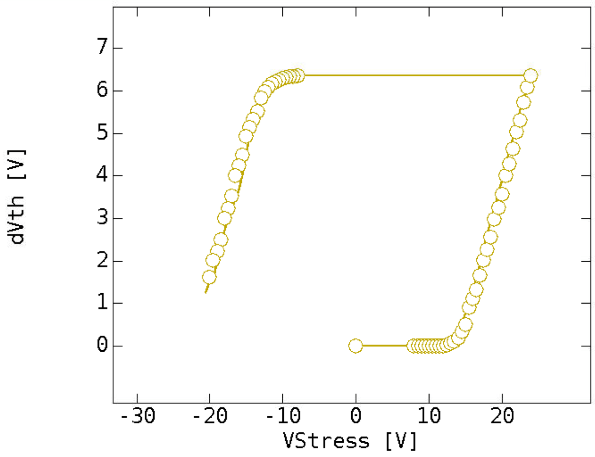
Using this model set, GTS Framework quantitatively predicts experimental ISPP, ISPE, and retention data with one common parameter set, accurately capturing the dependence of the program dynamics on the voltage of the control gate.
Cycling Degradation
Transconductance and charge trapping layer models can be combined with versatile and predictive oxide degradation models (insulator charging at point defects, trap-assisted tunneling) to describe non-ideal effects including increased retention loss and charge accumulation in the tunnel oxide. For the analysis of time-dependent variability and single-events, GTS Framework offers an advanced kinetic Monte Carlo engine.
GTS Minimos NT – simulate semiconductor devices and circuits: Run steady-state, transient, and small-signal analysis of arbitrary 2D and 3D device geometries. Combine multiple devices in a circuit with compact models. Run thermal analysys of devices and circuits.
GTS Nano Device Simulator – the first complete solution for effective physical simulation of nano-devices across technology nodes. Get profound predictive data for new materials and device architectures.
GTS Framework – the solid base of all GTS products and your working environment. Includes device editing, file management, distributed job execution, visualization, post-processing, a Python interface, etc.

