
23. July 2020
Pioneering for the 3nm node, GTS to present subband BTE solver with fully integrated source/drain-tunneling current calculation based on the WKB-approximation.
Source/Drain-Leakage becoming Issue Approaching the 3nm Node
As technology development progresses to the 5 nm-node and beyond, source/drain-leakage is found to be the ultimate obstacle to CMOS-scaling. In silicon, even with printed gate-lengths as low as 20 nm, intra-band source/drain-tunneling is not seen as a concern. However, this does not necessarily hold for alternative channel materials such as SiGe and Ge; both are considered candidates for the replacement of Si for high-performance CMOS at 3 nm. Such high-mobility materials come at the price of increased S/D-leakage.
SISPAD 2020: Fully Integrated Solution based on WKB Approximation
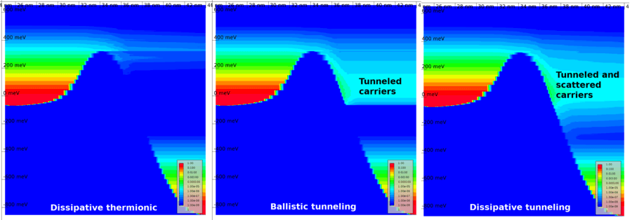
As part of the prestigious conference SISPAD 2020, Global TCAD Solutions (GTS) will be the first to present a paper describing a subband Boltzmann transport equation (BTE) solver with a fully integrated source/drain-tunneling current calculation based on the WKB-approximation.
The new method is validated against ballistic non-equilibrium Green’s function calculations showing good agreement with the latter. An investigation of Si and Ge-based nanowire-FETs is performed confirming that intra-band source/drain-tunneling is not a concern for Si devices. For Ge-based PMOS devices however, tunneling leakage limits sensible gate-length scaling.
Details
As the SISPAD 2020 will be a virtual conference, things will be different this year. Stay tuned for the scedule and details of our talk, or check the SISPAD web site.
Update: Find GTS’ paper in MyGTS here.