
19. March 2018
Presenting a Physical Modeling Study Based on 3D Phase-Space Subband Boltzmann Transport for Fully-Depleted SOI Technology
EuroSOI-ULIS: Physical Simulation of FD-SOI Technology
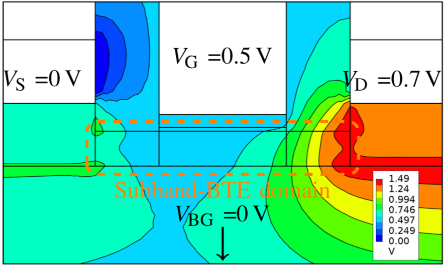
In their EuroSOI paper, GTS scientists present the first truly full-band approach to solving the subband Boltzmann transport (SBTE) equation in three-dimensional phase space. The solution is applied to investigate the evolution of the FD-SOI MOSFET towards the 7nm node. Findings show that single-gate FD-SOI technology can be effectively scaled down to the 14nm node, because the on-current gains are large enough to offset the SS-degradation. Beyond 14nm, a double-gate thin-body geometry is required to maintain electrostatic control.
The paper is presented at EuroSOI-ULIS 2018, at the University of Granada, on Wed march 21, in session 9.


The images compare characteristics of two consecutive technology nodes (22nm vs. 14nm and 10nm vs. 7nm), respectively.
The respective new feature, allowing physical modeling of ultra-scaled FD-SOI technology, such as double-gate MOS transistors, is available in GTS Nano-Device Simulator (NDS) within GTS Framework 2018.03.