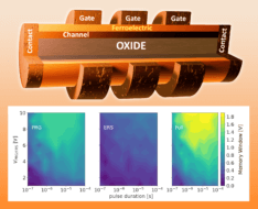
GTS @ ESSDERC 2023: Ferroelectric VNAND Memory
Combine the competing effects of ferroelectricity and charge trapping in a single simulation work-flow in GTS Framework – nicely matching experiment results from literature.
To narrow your search, add more words.
Example queries: dtco / subband boltzmann / finfet tutorial / vnand example / degradation publication ieee
Combine the competing effects of ferroelectricity and charge trapping in a single simulation work-flow in GTS Framework – nicely matching experiment results from literature.

GTS presenting novel semi-analytical model for wave-function penetration, resolving long-standing problems such as carrier spillover and large errors in surface roughness scattering.

GTS CTO Zlatan Stanojević is chairing session Simulation & Modeling of Defects & Traps together with Denis Rideau (STMicroelectronics) — Thursday September 16, 2021 (16:00-17:00)
We are looking forward to seeing you at ESSDERC 2019 in Kraków: Our CTO Zlatan Stanojević will be chairing session C2L-G “Multi-physics Modeling” (Track 3), together with Viktor Sverdlov.
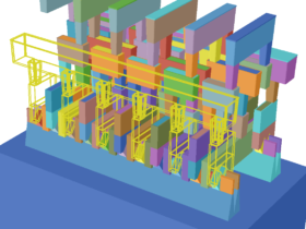
GTS presenting first practical TCAD-based work flow for design-technology co-optimization (DTCO) of standard cells.
We present novel models for insulator wave-function penetration and for interface roughness scattering. We review the intricate relationship between modeling of these two effects, with respect to usability, computational effort, and numerical stability. We demonstrate that our novel approach is capable of remedying all of the common issues of previous approaches at no additional computational cost.

1 MB
We present the first practical TCAD-based work flow for design-technology co-optimization (DTCO) of standard cells. The flow consists of parametric cell layout templates, layout-based structure generation, mixed-mode transient electri- cal device simulation, and data collection and analysis. Based on electrical and structural characterizations of the iN14, iN10, and iN7 nodes, the models presented in this work feature a projection for 5nm technology nodes based on FinFET, nanowire, and nanosheet. Transient five-stage ring-oscillator simulations show a clear advantage for the FinFET in terms of switching frequency and power consumption.
1 MB
We present a simulation modeling chain for nano-scaled III/V quantum-well MISFETs. Our methods are based on physical rather than empirical modeling, which allows to obtain predictive simulation results with very few fitting parameters. We use a recent InGaAs-based technology from Intel [1] to validate our simulation results which show excellent agreement with measured capacitance and conductance curves. We further evaluate the properties of a 60 nm long InGaAs quantum-well transistor, finding a sub-threshold slope of 73.5 mV/dec and a DIBL of 103.8 mV/V. A fast numerical computational framework ensures high modeling flexibility; at the same time execution times are kept short making our approach an ideal replacement for empirical device modeling which is still pervasive in TCAD.
< 1 MB
With our suite of physical modeling tools for path-finding (including Minimos-NT, VSP, and NDS), you can easily, safely, and cost-effectively find your path to technological superiority. Get Accurate Results for Each Device Architecture Being able to precisely predict and compare device performance significantly cuts the need for costly and time-consuming experiments. To get predictions that … Continued
Research-based, European TCAD