
High-performance computing (HPC), artificial intelligence (AI) and neuromorphic applications, millimeter wave 5G/6G technology, quantum computing, cryogenic electronics, and power electronics are steadily pushing the semiconductor technology beyond the physical limits of silicon. Research into novel materials and device concepts bears high risks but offers great rewards of disruptive technological breakthroughs. GTS VSP, Minimos-NT, NDS, and NDS Atom assist you in making the right decisions and are the right tools to put you ahead of your competition.
New Materials
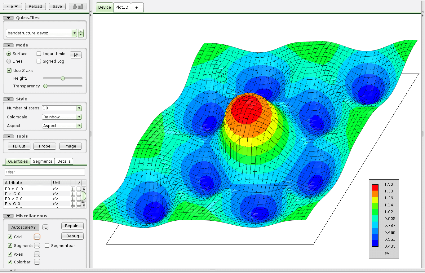
Transition metal dichalcogenides (TMD) can be exfoliated to form atomic monolayers of semiconductor material. True two-dimensional semiconductors consisting of one or few atomic layers of TMD material represent the ultimate form of confinement of carrier confinement. Combined with their low defect density they present the ultimate electrostatic channel control for low-power applications. VSP and NDS Atom allow easy and efficient evaluation of prototypical TMD-based devices, leveraging results obtained directly from ab-initio methods.
Carbon nanotubes (CNT) and graphene with their extremely high carrier mobility seem like a good proposal for fast-switching high-performance applications. However, their small band gap and low effective mass makes them susceptible to leakage. With its integrated WKB and BTE solvers, NDS Atom can predict ballistic transport, tunneling, and scattering in these materials and help avoid their shortcomings in device design.
III-V, III-Nitride materials, and SiC offer bandgaps and carrier mobilities vastly different from silicon, making them interesting for applications where high breakdown-voltage, high mobility, or a direct optical transitions are desired, such as power electronics, RF, or optoelectronics. Unlike silicon however, these materials suffer from low gate oxide reliability. Minimos-NT, VSP, and NDS provide the right models to tackle carrier trapping and device degradation in these material systems.
New Devices
The advent of gate-all-around (GAA) architectures as well as 2D and 1D materials, such as TMD monolayers and CNTs has introduced fully confined transport, which opens new possibilities for device concepts.
Junctionless FETs eliminate the need for p/n-junctions by using the gate to deplete the channel of carriers, thus allowing them to operate as efficiently as MOSFETs, while keeping carriers away from the gate oxide where they might scatter of become trapped.
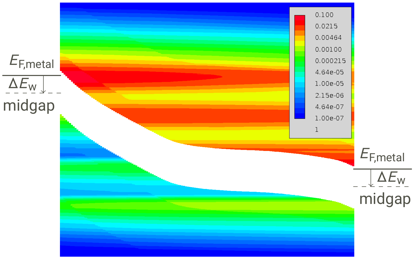
Schottky-FETs replace the conventional ohmic contacts with Schottky (metal-semicondcutor) contacts. Apart from the doping the metal work function can be used to control carrier injection through thermionic injection and tunneling.
By placing additional gates around the source and drain contacts, junctionless Schottky FETs can become reconfigurable ambipolar FETs, that can be electrically switched between NMOS and PMOS.
Tunnel FETs inject cold carriers into the channel via band-to-band tunneling, thus avoiding Boltzmann’s tyranny that imposes a lower limit on the sub-threshold swing of classical FET devices.
Ferro-electric FETs (FeFETs) enhance a device’s operation by using a ferro-electric high-k layer, which adds a memory function to the device.
One Solution
GTS Framework and the simulators within (Minimos-NT, VSP, NDS, NDS Atom) provide an integrated platform for exploring new materials as well as designing and optimizing new devices. The tools specifically support this kind of tasks through their unique features:
- Built-in effective mass and k·p band structure models for most semiconductors and graphene/CNTs
- Import and direct use of DFT-generated band structures for mobility and transport calculations as well as extraction of parameters such as effective masses from ab-initio data
- Boltzmann transport equation (BTE) and drift-diffusion (DD) solvers with integrated WKB-based models for intra-band, band-to-band, and Schottky barrier tunneling
- Support for various scattering mechanisms: phonons, (remote) Coulomb scattering, surface roughness
- High flexibility regarding device geometry: arbitrary contact geometries, multiple gates and oxides, doping, etc.
- Rich and easily extendable material database
- User-friendly interface and short turn-around times ensure high productivity
GTS Nano Device Simulator – the first complete solution for effective physical simulation of nano-devices across technology nodes. Get profound predictive data for new materials and device architectures.