
Profound Physical Device Simulation
![]()
GTS Nano-Device Simulator (NDS) is the first fully integrated solution for effective physical simulation of nano-scale MOSFETs independent of their technology nodes. NDS is built around a solver for the subband Boltzmann transport equation and provides complete coverage of short-channel effects, including velocity overshoot and source-drain tunneling. NDS is the tool of choice for profound predictive simulation of current and future CMOS technologies.
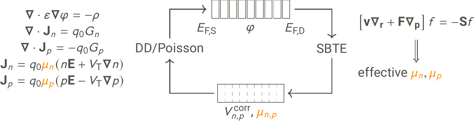
NDS is an advanced device simulation tool based on the solution of the subband Boltzmann transport equation (SBTE) in a critical region of the device such as the channel. NDS incoroprates the electrostatic and near-equilibrium transport from Minimos-NT, and the subband structure calculation and scattering models from VSP. It further extends the SBTE with tunneling transport based on the WKB approximation. As such, NDS can accurately account for material characteristics, crystal orientation, stress, quantum effects, ballistic and kinetic (non-equilibrium) transport effects, all in one package based on solid physical background. The integration with the classical simulator Minimos-NT provides flexibility, stable convergence, and ease-of-use. Despite its sophisticated physical models NDS can be operated just like a classical drift-diffusion-based simulator.
NDS can efficiently simulate the whole range of device characteristics using just one simulation setup and run. In this way, the user can obtain both accurate and fast device simulation results for various device architectures, materials and bias points.
NDS accounts for all physical phenomena relevant for operation, performance, and reliability of nano devices, such as material characteristics, crystal orientation, stress, ballistic effects, scattering, direct tunneling, band-to-band tunneling, etc. In one single simulator setup, NDS can predict transistor performance parameters like electron mobility, ION, IOFF, sub-threshold slope, DIBL, leakage, and more — all based on physical simulation relying on material properties rather than empirical models. At the same time, NDS simulations have short turn-around times that make it well-suited for day-to-day use in TCAD.
Capabilities
Drive Current (ION)
- Boltzmann transport equation
- Ballistic and dissipative transport
- Velocity overshoot
- Quantum resistance
- Performance enhancement by channel strain
Off-state Leakage (IOFF)
- Quantum-mechanical transport
- Direct SD-Leakage
- Band-to-Band Source-Drain leakage
Models
NDS leverages the microscopic models available in VSP and combines them with a phase-space transport (PST) solver to solve the SBTE. By using the same band structure and scattering models as VSP, NDS makes it possible to cross-calibrate and transfer model parameters between the two tools – see model building in path-finding for silicon.
Band Structure
Models are consistent with the ones used in VSP.
- Effective mass approximation (EMA) or k·p-based Hamiltonians
- Quantum confinement giving rise to subband structure
- Arbitrary crystal orientations
- Responds to mechanical stress through deformation potentials
Scattering
Models are consistent with the ones used in VSP.
- Acoustic phonon scattering
- Optical and inter-valley phonon scattering
- Polar-optical phonon scattering
- Surface roughness scattering
- Coulomb scattering from local and remote sources (dopants, oxide charges and dipoles, traps)
- Alloy disorder scattering
Phase-Space Transport
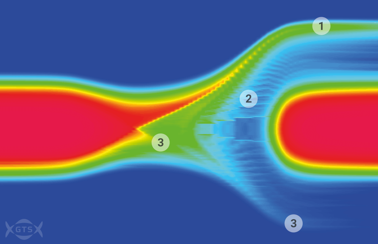
- Solution of coupled mulit-subband BTE in r–k-space, i.e. phase space for electrons and holes
- Electron/hole distribution function of position, momentum, and energy gives detailed insights into device operation at any bias
- Semi-classical transport: ballistic transport & scattering
- Pauli-exclusion, Fermi-Dirac statistics
- Crystal orientation and strain effects automatically included through subband structure
- Multi-dimensional: planar and non-planar devices
- Adaptive r, k, and energy grids for maximum simulation performance
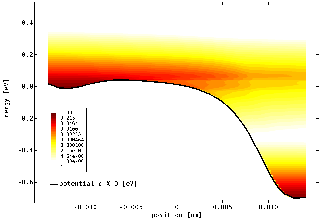
Tunneling Transport
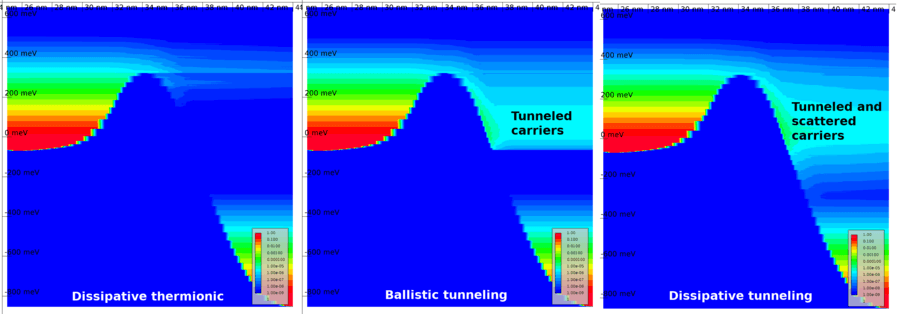
- Intra-band source-drain tunneling, Schottky-barrier tunneling, band-to-Band tunneling
- Transmission coefficients computed using WKB approximation
- Based on numerical computation of complex (sub-)band structure
- Seamless integration of tunneling rates within PST
- Tunneling included in PST with virtually no added run-time or memory cost
- Accuracy verified against ballistic NEGF
Environment
- Integration in the GTS Framework
- Graphical user interface
- Sophisticated input-deck database
- Multi-core simulation support
- Material database extendable via C++ like script language
- Import of third-party device geometries and meshes
Beyond Silicon
NDS Atom is a device simulation tool specialized to novel material systems and device concepts that combines the benefits of NDS with
- Capability of simulating two-dimensional semiconductors
- Interoperability with ab-initio calculations: electronic structure import, effective mass extraction, use of ab-initio-based electron-phonon couplings
- Models for thermionic and tunneling carrier injection from Schottky contacts – both side-contacts and wrap-around contacts
- Improved BTE solver kernel to tackle both short and long-channel devices


Sound Choice for New Challenges
True physical simulation is the only way of getting profound data for device shrinking, and for designing, optimizing and predictively evaluating new device architectures and new materials. As a unique, well-maintained, modular and expandable physical modeling platform but one which can deliver accurate results in reasonable time, GTS Nano-Device Simulator is the sound choice for years to come.